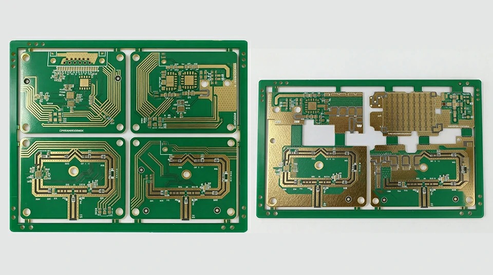
Precision PCB Fabrication with Verified Manufacturing Capability
LinkPCBA provides professional PCB manufacturing services focused on precision fabrication, stable process control, and long-term production reliability.
Rather than presenting theoretical limits, our PCB manufacturing capability is defined by qualified production parameters and validated engineering processes, ensuring designs can transition smoothly from prototype builds to stable mass production.
PCB Manufacturing Technical Capability Overview
Category | Specification | Capability / Range |
|---|---|---|
Layer & Size | Layer Count | 1–30 layers (Prototype) / 1–20 layers (Mass Production) |
Layer & Size | Max Board Size | 570 × 850 mm |
Layer & Size | Board Thickness | 0.13 – 7.0 mm |
Layer & Size | Aspect Ratio | Up to 12:1 |
Copper & Stack-Up | Copper Weight | Inner: 1/3–6 oz / Outer: 1/2–6 oz |
Copper & Stack-Up | Hybrid Stack-Up | FR-4 + RF / FR-4 + Metal Core |
Line & Space | Min Line / Space | Down to 3 / 3 mil (by copper class) |
Drilling & Vias | Mechanical Hole | 0.1 – 6.2 mm |
Drilling & Vias | Laser Via | ≥0.1 mm (Depth ≤65 μm) |
Drilling & Vias | Blind / Buried Vias | Supported |
Impedance Control | Impedance Tolerance | ±5 Ω (<50 Ω) / ±10% (≥50 Ω) |
Materials | Standard & High-TG FR-4 | Shengyi, KB, ITEQ, FR408, IT180A |
Materials | High-Frequency / RF | Rogers, Taconic |
Materials | Metal Core | Aluminum / Copper |
Surface Finish | Available Finishes | HASL (LF), ENIG, ENEPIG, OSP, Imm. Silver/Tin |
Plating Control | Gold Thickness | 0.03 – 0.1 μm |
Solder Mask | Mask Colors | Green, Matte Black, Blue, Red, White |
Solder Mask | Min Mask Bridge | 4 mil |
Accuracy | Hole Position Tolerance | ±0.076 mm |
Accuracy | Board Outline Tolerance | ±0.1 mm |
Testing | Electrical Test | 100% E-Test (Flying Probe / Fixture) |
Compliance | Standards | IPC-A-600 / IPC-6012, RoHS, REACH |
- 1
- 2
- 3
All specifications listed in the table represent production-proven capabilities, released through internal engineering validation and quality control procedures.
Capability availability may vary depending on material system, copper weight, and stack-up complexity.
What PCB Manufacturing Means at LinkPCBA
At LinkPCBA, PCB manufacturing is approached as a manufacturing discipline, not a specification showcase.
Our focus is on:
- Manufacturability at scale
- Process repeatability across batches
- Dimensional and electrical consistency
- Long-term supply stability
Every PCB design is reviewed from a manufacturing-first perspective, reducing yield risk and unexpected variation during volume production.
Materials, Stack-Up & Process Control
We support a broad range of standard, high-performance, and application-specific PCB materials, including FR-4, high-TG, halogen-free, high-frequency RF, and metal-core substrates.
Material selection and stack-up design are evaluated based on:
- Electrical performance requirements
- Thermal and mechanical constraints
- Reliability expectations
- Long-term material availability
All fabrication processes are executed under controlled conditions to maintain dimensional accuracy, copper integrity, and impedance consistency.
Quality Assurance & Traceability
Quality control is embedded throughout the PCB manufacturing process, including:
- Incoming material verification
- In-process inspection at critical stages
- 100% electrical testing prior to shipment
- Batch-level traceability supported by MES systems
Our PCB manufacturing operations comply with applicable IPC standards, as well as RoHS and REACH environmental requirements.
Advanced PCB Manufacturing Support
In addition to standard multilayer boards, LinkPCBA supports advanced PCB manufacturing requirements such as:
- HDI and blind/buried via structures
- Impedance-controlled designs
- Back drilling and via filling
- High-frequency and mixed-material stack-ups
- Metal-core PCBs for thermal management
Advanced features are evaluated based on design feasibility and production validation, not theoretical capability claims.
Application Scenarios
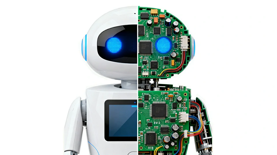
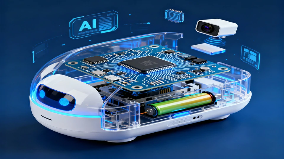
AI Intelligence
Security System
Automotive electronics
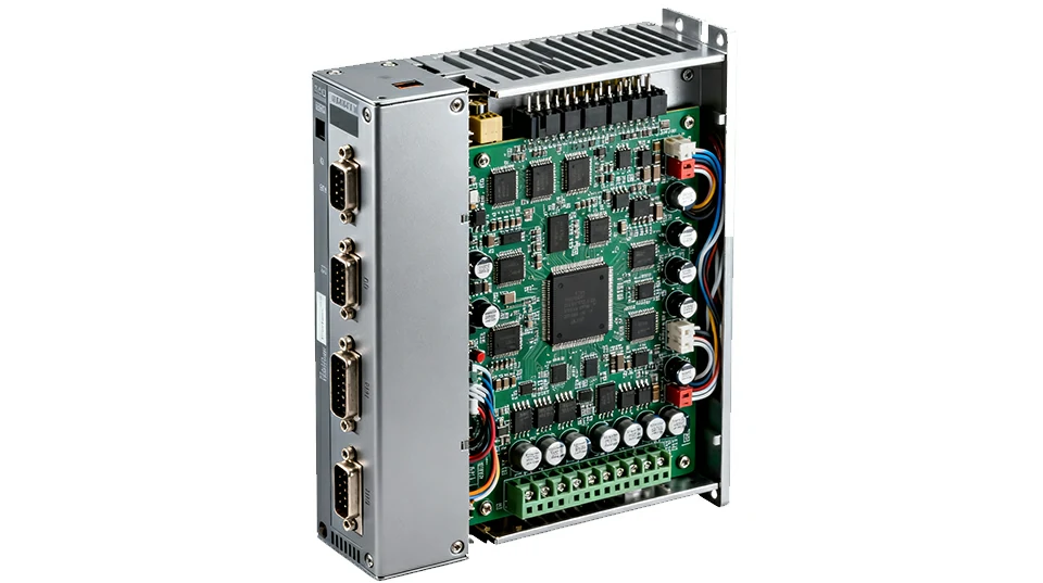
Industrial control
Medical devices
IoT & smart devices
New energy & power systems
Security & Communication Systems
Stable and interference-resistant PCBA for surveillance, access control, and communication infrastructure. Designed for 24/7 operation with EMC protection, shielding, and long-term component reliability.
Automotive Electronics
Precision PCBA manufacturing for automotive control units, ADAS systems, and EV battery management. All assemblies meet IPC Class 3 and IATF16949 standards for vibration resistance and long-term reliability.
Industrial Control Systems
Durable PCBA solutions for automation, robotics, and power management. High-temperature and high-current designs are validated through AOI, X-Ray, and functional testing to guarantee stability in demanding environments.
Medical Devices
Certified ISO13485 manufacturing for diagnostic, monitoring, and portable medical electronics. Every production stage follows traceable quality control to ensure safety, accuracy, and compliance with global medical regulations.
IoT & Smart Devices
Compact, energy-efficient assemblies for IoT modules, wearables, and smart-home systems. RF optimization and multi-protocol compatibility (Wi-Fi, BLE, LoRa) deliver reliable connectivity in small-form designs.
New Energy Systems
Reliable PCBA manufacturing for renewable energy applications, including solar inverters, energy storage systems, and EV charging infrastructure. Boards are designed for high current, heat resistance, and long operational lifespan under continuous load.
Why Choose LinkPCBA for PCB Manufacturing
Customers choose LinkPCBA because we provide:
- Clearly defined and verified PCB manufacturing capabilities
- Stable quality performance from prototype to mass production
- Engineering-driven manufacturing decisions
- Transparent process control and traceability
- Long-term production reliability rather than short-term capability claims
We act as a manufacturing partner, not a specification reseller.
FAQ — PCB Manufacturing
Yes. All listed capabilities are based on qualified production parameters designed to support both prototype builds and volume manufacturing.
Yes. Custom stack-up design and impedance control are supported based on material selection and manufacturing feasibility evaluation.
Yes. Every PCB undergoes 100% electrical testing prior to shipment.
Consistency is maintained through controlled process windows, material traceability, and ongoing quality monitoring.
Yes. Advanced PCB technologies are supported following engineering review and production validation.
Start Your PCB Manufacturing Project
If you are looking for a PCB manufacturing partner with verified capabilities, controlled processes, and long-term reliability, LinkPCBA is ready to support your project.
Contact us to discuss your PCB manufacturing requirements or request a technical review.
⭐ Updated April 2025 — Reviewed by LinkPCBA Engineering Team