IoT Devices & Smart Home PCB / PCBA Manufacturing
IoT and smart home electronics require compact design, stable wireless performance, low power consumption, and reliable mass-production capability. LinkPCBA provides complete PCB and PCBA manufacturing solutions for smart sensors, edge devices, connectivity modules, smart home controllers, wearable IoT devices, gateways, and low-power embedded systems.
With three Shenzhen manufacturing centers and an integrated one-stop workflow—from PCB fabrication to SMT, DIP, testing, and final assembly—we support global IoT OEM & ODM customers with fast prototyping, stable mass production, and strong engineering support.
Customer Project Scenario — Compact & Wireless IoT Systems
A smart home device developer partnered with LinkPCBA to create a multilayer PCBA used in a Wi-Fi / BLE connectivity module.
The project required:
- Compact HDI layout for portable IoT form factors
- Stable Wi-Fi, BLE, Zigbee, or LoRa wireless performance
- Low-power design for battery-driven devices
- Accurate antenna tuning and RF layout optimization
- Quick prototype iterations for product refinement
- Smooth scaling into mass production within weeks
LinkPCBA delivered a fully validated IoT manufacturing solution enabling fast prototyping, RF performance tuning, and stable large-scale production.
Technical Challenges in IoT Electronics
IoT devices face tight design constraints and require optimized wireless performance. Key challenges include:
- Small form factor & HDI density
IoT devices require fine-pitch components, tight layouts, and multi-layer HDI structures. - Wireless signal integrity
RF layout, antenna design, grounding, and isolation must be precise for stable connectivity. - Low-power consumption requirements
Battery-driven IoT devices need efficient routing, low-leakage materials, and optimized power paths. - Mixed RF + digital + analog circuits
IoT boards often combine sensors, wireless chips, and microcontrollers. - Fast development cycles
IoT hardware requires rapid prototyping and multiple quick iterations.

LinkPCBA Manufacturing Solution for IoT Devices
Engineering Support
DFM & DFA for compact IoT layouts
RF routing, antenna tuning, and impedance optimization
Low-power design guidance
Sensor accuracy and stability optimization
EMI/EMC improvement for FCC/CE compliance
PCB Manufacturing
HDI, 4–10 layer IoT PCBs
Controlled impedance for RF sections
High-precision LDI imaging
High-quality ENIG / ENEPIG finishes for RF pads
Compact footprints for portable devices
PCBA Assembly
High-precision SMT for fine-pitch IoT components
BGA, QFN, 0201 mixed assembly
RF modules, sensors, MCU, PMIC assembly
AOI, SPI, and X-ray testing
Conformal coating for environmental protection
Wireless / Functional Testing
RF performance validation
Antenna tuning & S-parameter checks
Functional IoT protocol testing
Burn-in testing for long-term reliability
IoT Production Capability
With three Shenzhen manufacturing centers, LinkPCBA supports:
- Prototype → NPI → Mass production
- Rapid 24-hour prototypes
- Full wireless testing support
- Fast ECN modifications
- Stable supply chain for MCUs, sensors, RF chips
We ensure stable long-term production for global IoT clients.
IoT Application Segments We Support
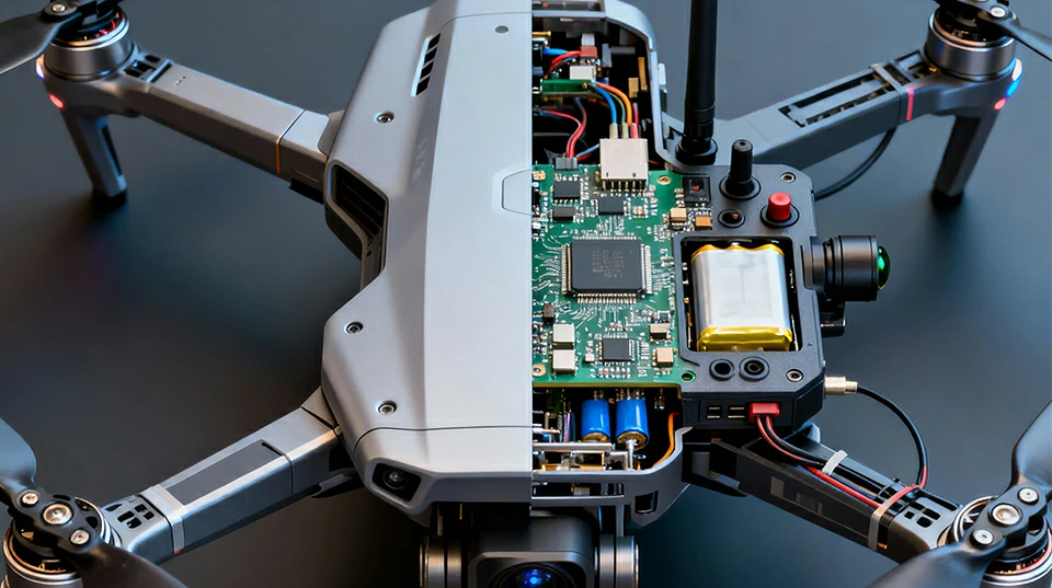
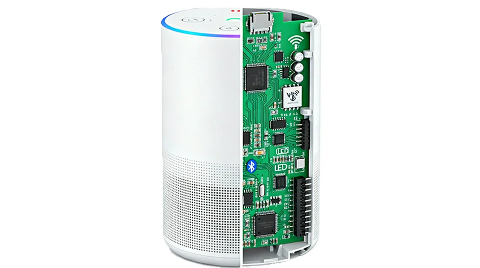
Smart Home Devices
Smart switches, controllers, lighting, home automation modules
Wireless Connectivity Modules
Wi-Fi, BLE, Zigbee, Z-Wave, LoRa modules
Portable & Wearable Devices
Smart trackers, health wearables, mini embedded IoT gadgets
Smart Sensors
Temperature, humidity, motion, vibration, proximity sensors
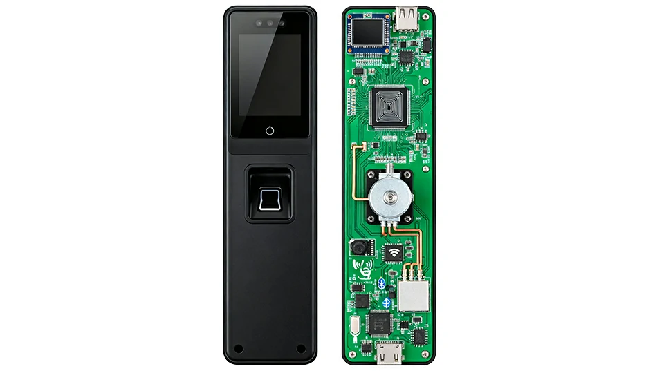
Edge Computing & Miniature AI Devices
Low-power AI modules, micro-controllers, intelligent sensor nodes
Smart Industry & Commercial IoT
Gateways, data collectors, wireless monitoring devices
Why OEM & ODM Clients Choose LinkPCBA for IoT Manufacturing
- Strong RF & antenna engineering capabilities
RF optimization for Wi-Fi / BLE / Zigbee / LoRa. - Ultra-compact IoT design expertise
HDI PCBs, fine-pitch SMT, and optimized layouts. - Fast prototyping and fast iterations
24-hour sample builds and rapid ECN updates. - One-stop manufacturing solution
PCB + SMT + DIP + testing + assembly. - Wireless testing & compliance support
RF validation, antenna tuning, and EMI/EMC improvement.
Case Study — Smart Home Wi-Fi/BLE Module
A customer required a compact wireless module for a smart home gateway.
LinkPCBA delivered:
- 4-layer HDI PCB
- Optimized antenna & RF line routing
- Mixed 0201 / QFN / RF components assembly
- Full wireless performance testing
- Stable mass-production scaling
The final product passed FCC/CE wireless testing and shipped globally.
FAQ — IoT Devices PCB / PCBA
Yes. We provide RF engineering support and wireless performance validation.
Yes. We specialize in HDI and miniature IoT designs.
Yes. We offer functional testing and RF validation.
Yes. Our engineering team optimizes power paths and signal routing.
Yes. We provide 24-hour samples and fast ECN processing.
Start Your IoT Device Project
LinkPCBA delivers reliable, compact, and wireless-optimized PCB & PCBA manufacturing for global IoT products.
Our engineering team responds within 24 hours for DFM, RF optimization, and quotation.
⭐ Updated April 2025 — Reviewed by LinkPCBA Engineering Team